

Instrument
Contact
Tel. +30 2610 965522

Scanning Electron Microscope (SEM / EDS / EBSD)
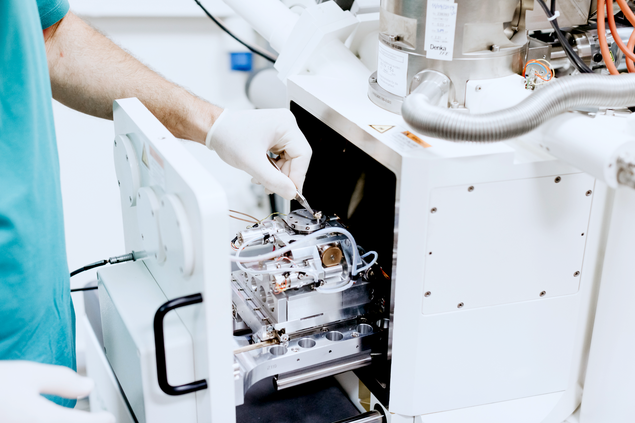
Scanning electron microscopy (SEM) is a well-known technique for the morphological characterization of materials. In SEM, a finely focused electron beam with energy of 30kV scans over a sample surface and the secondary, backscattered electron etc. are emitted from the surface. The intensity of the emitted electrons is sensitive to the topographic features of the sample surface. The signals are collected from a detector and amplified. The variation of the resulting signal strength varies the brightness the trace of a CRT that is scanned synchronously with the electron beam. The image of the surface is thus displayed on to the CRT screen.
Elemental chemical analysis can be performed in a SEM microscope by measuring the energy or wavelength distribution of the X-ray signal generated by the electron beam. For this purpose, the SEM microscope is equipped with an EDS analyser allowing for semiquantitative and quantitative chemical analysis. Also phase imaging and orientation imaging can be measured with HKL EBSD system that is added on the microscope
Characteristics
Scanning electron microscopy (SEM) is a well-known technique for the morphological characterization of materials. In SEM, a finely focused electron beam with energy of 30kV scans over a sample surface and the secondary, backscattered electron etc. are emitted from the surface. The intensity of the emitted electrons is sensitive to the topographic features of the sample surface. The signals are collected from a detector and amplified. The variation of the resulting signal strength varies the brightness the trace of a CRT that is scanned synchronously with the electron beam. The image of the surface is thus displayed on to the CRT screen.
Elemental chemical analysis can be performed in a SEM microscope by measuring the energy or wavelength distribution of the X-ray signal generated by the electron beam. For this purpose, the SEM microscope is equipped with an EDS analyser allowing for semiquantitative and quantitative chemical analysis. Also phase imaging and orientation imaging can be measured with HKL EBSD system that is added on the microscope
Services
Model: Zeiss SUPRA 35VP
Electron Gun: FE
Resolution: 1,7nm at 20kV (HV)|2,0nm at 30kV (LV)
Image Detectors: ET-SE, VPSE, Inlens-SE, BSE
Element indentification: C-U
Quantitative analysis:
Point (standard)/line/map (standardless)
Phase imaging, Orientation imaging
Texture analysis
Sample Properties
Powders, pellets, solids
Max height: 25mm
Weight: less than 0.5 Kg