Publication
Signatures of Quantized Energy States in Solution-Processed Ultrathin Layers of Metal-Oxide Semiconductors and Their Devices

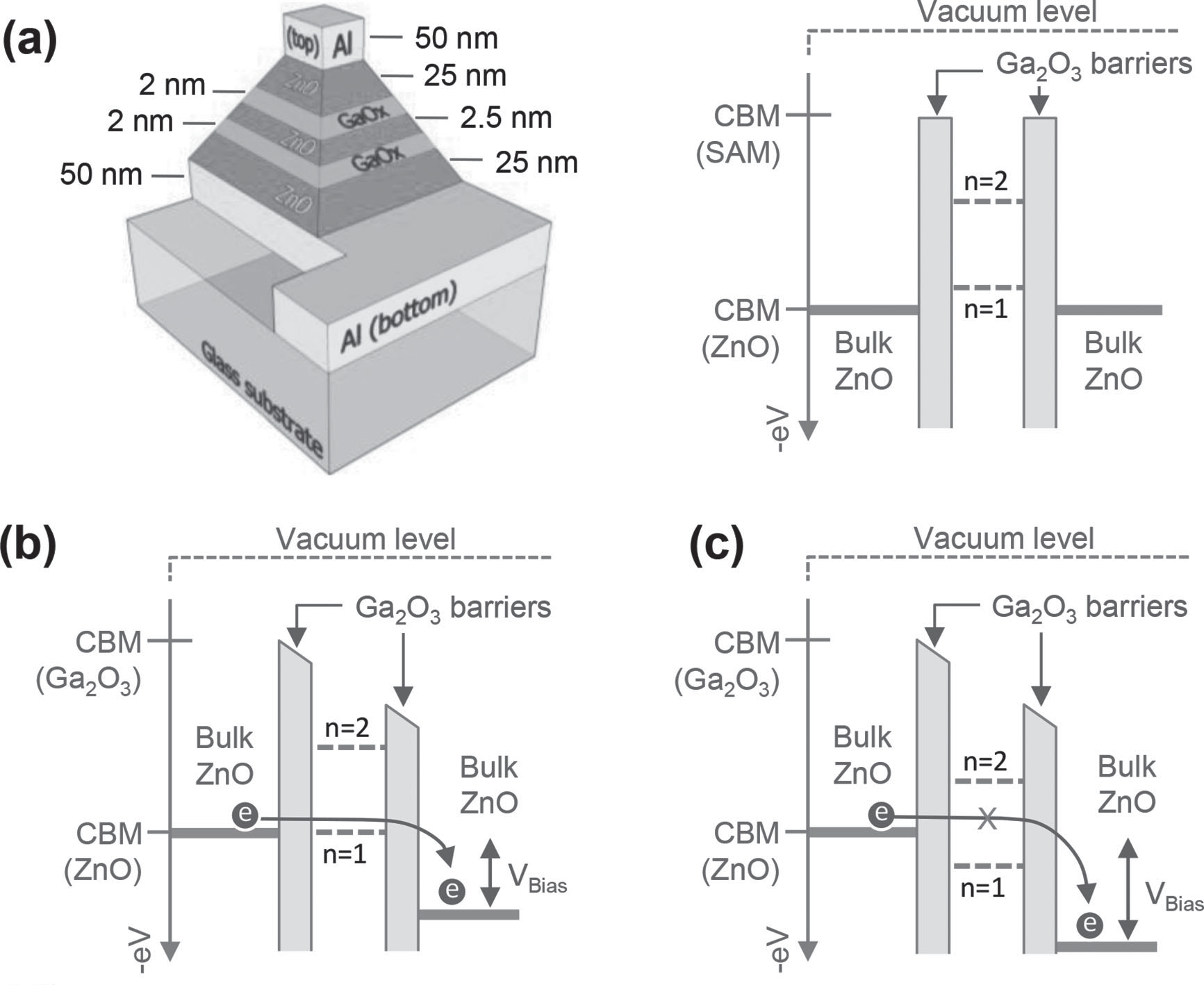
a) Schematic representation of the solution-processed ZnO resonant tunnelingdiode (RTD) structure developed and the idealized energy band diagram under zero bias. The RTD consists of a central quantum well, formed of an ultrathin (∼2-3 nm) ZnO layer confined between two ultrathin (∼2 nm) Ga 2 O 3 barrier layers. The quantum well structure is enclosed between two bulk (25 nm-thick) ZnO layers on either side, which are in direct-contact with aluminum electrodes (labeled Al). b,c) Idealized representation of conduction band of solutionprocessed resonant tunneling-diode under two biasing conditions. The labels n n=1 and n=2 represent the discreet energy levels of the central ZnO semiconductor. The labels on the y -axis "CBM (Ga 2 O 3 )" and "CBM (ZnO)" represent the energies of the conduction band minima of the Ga 2 O 3 barrier layers and ZnO bulk layers, respectively
Journal: ADVANCED FUNCTIONAL MATERIALS
Year: 2015
Volume: 25
Issue: 11
Pages: 1727-1736
https://doi.org/10.1002/adfm.201403862
https://doi.org/10.1002/adfm.201403862
11.8


